Electronics/Op-Amps
Amplifiers
Op-Amp (operational amplifier)
Remember when we talked about "ideal" capacitors and inductors, but then discussed all the imperfections of real capacitors and inductors? We're going to do the same thing here, except 3 times instead of twice.
- Designing op-amp circuits
- Ideal op-amps
- technical details about non-ideal op-amps
The idea of an "ideal" op-amp makes it easier to design circuits. Later we will discuss the various ways that real op-amps fail to work as we expected.
An operational amplifier or op-amp is an electronic circuit module, which has a non-inverting input (+), an inverting input (-) and one output.
Originally, op-amps were so named because they were used to model the basic mathematical operations addition, subtraction, integration, differentiation etc in electronic analog computers. In this sense a true operational amplifier is an ideal circuit element.
An example
See Wikipedia:Operational amplifier and look for the "Internal circuitry of 741 type op-amp" section. See also the data in the Linear Databook published in 1982 by the National Semiconductor Corporation.
- This particular op-amp requires either two supply-voltage sources of never more than (18 volts(V) for 741C), (22V for 741, 741A and 741E) each, or a center/centre tapped equivalent voltage source with each half supplying never more than the same voltage.
- The maximum permitted power dissipation is 500 milliWatt(mW).
- The maximum input voltage must never be more than 15V, with the maximum permitted differential voltage being 30V.
- The maximum storage temperature range permitted for all these op-amps is minus 65 degrees Celsius to plus 150 degrees Celsius.
- The actual operating ambient temperature for 741C and 741E is zero to 70 degrees Celsius, and it is minus 55 degrees Celsius to plus 125 degrees Celsius for 741 and 741A.
- For the many additional data see the Linear Databook.
Another example
The Linear Databook, among data for also many other types, lists information, for example, about nearly equal types 124, 124A, 224, 224A, 324, and 324A op-amps from page 3-172 to 3-180. Their special advantage is that only one power supply is needed, and that there are 4 op-amps in a single dual-in-line package.
- Electrical characteristics are listed from pages 3-173 to 3-174, mainly for a more usual single supply voltage of plus 5 V.
Notation
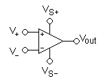
A typical circuit symbol for an op-amp looks like this:
Its terminals are:
- V+: non-inverting input
- V−: inverting input
- Vout: output
- VS+: positive power supply
- VS−: negative power supply
Often these pins are left out of the diagram for clarity, and the power configuration is described or assumed from the circuit.
The input pin polarity is often reversed in diagrams for clarity. In this case, the power supply pins remain in the same position; the more positive power pin is always on the top, and the more negative on the bottom. The entire symbol is not flipped; just the inputs.
Quick Design Process
Imagine we have a (weak) input signal, and we want to amplify it to generate a strong output signal; or we have several different voltages, and we want to add them together. For these purposes, we need op-amp amplifying and summing circuits. It seems that there is nothing new to say about these bare (usually single op-amp) circuits. Only, the innovator Dieter Knollman has suggested a new simpler design procedure in an EDN's article [1]. He has also placed his work on the web[2] (see also a circuit story[3] written after Dieter's work).
We assume:
- All inputs are ideal voltage sources.
- Gain is defined as the gain from the ideal voltage source to the op-amp output.
- The feedback resistor, Rf, connects from the op-amp output to the inverting input.
- The input resistor, Ri, connects from the ideal voltage source input to the op-amp input. (This *includes* any source resistance).
- positive-gain inputs connect (through that resistor) to V+
- negative-gain inputs connect (through that resistor) to V−
Design procedure:
- First, specify the desired circuit gains for each input.
- Then calculate the ground gain, as follows:
- Daisy's theorem:
- The sum of the gains = +1 in a properly-designed op amp circuit.
Therefore, choose
- Ground gain = 1 - ( the sum of the desired positive and negative gains).
- Choose a feedback-resistor value. For example, let Rf=100 kiloOhms.
- Next, calculate the resistor values for each input, including the ground-gain resistor, using
- .
- where |gain| is the absolute value of the desired gain.
Some op-amp circuits need a resistor to ground from the op amp's inverting input.
Others need a resistor to ground on the noninverting input.
The sign of the ground gain determines where to place the ground resistor.
If the desired gains add up to one, a resistor to ground is unnecessary.
You will see below some examples that illustrate using the quick design procedure. First of all, answer the question, "What's the highest and lowest output voltage you want?" Make sure the power terminals of the op-amp are at least that high and low. (If you want it to swing from +5V to -5V, then an op-amp connected to 0V and +10V won't work).
Ideal Op Amps
The output voltage is the difference between the + and - inputs multiplied by the open-loop gain: Vout = (V+ − V−) * Avo.
The ideal op-amp has an infinite open-loop gain, infinite input impedances and zero output impedance. The input impendance is the impedance seen between the non-inverting and inverting inputs.
The model for the Op Amp is shown in Figure 1. Where V+ − V− is equal to vd; Rin is the input impedance; Rout is the output impendance; Avo is the open loop gain; and Rs is the source impedance.
- Figure 1: The model of the Op Amp.
Using voltage divider rule, we can determine the voltage vd.
- (1)
Since the dependent voltage source amplifies the voltage vd by Avo. We can work out the output voltage across RL once again using voltage divider rule.
- (2)
Substituting equation 1 into 2.
Now if the properties of an Ideal Op Amp are applied. The ideal properties of an Op Amp are infinite input impedance and zero output impendance. Since Rin >>, much greater than, Rs, Rin/(Rin+Rs) 1.
Which is basically the definition of an Op Amp. But if the input impendance was not infinite and the output impendance nonzero then this would not be so.
Basic Op-Amp Configurations
All the more complicated Op Amp configurations are based on two basic ones; the Inverting and Non Inverting configurations. An understanding of these two configurations, makes it much simpler to understand the more advanced configurations.
Inverting Op Amp
The closed loop gain of an Inverting Op Amp is
- (i)
Input Impedance of this configuration is Zin = Rin (because V− is a virtual ground, no current flows into the Op Amp ideally.)
To get formula (i) we take a KVL loop with , and the inputs of the Op Amp. This gives
Where is the voltage between the non-inverting and inverting inputs. But for ideal Op Amps is approximately zero. is zero because the input impedance is infinite, which means the current through the impedance must be zero by Ohms law. The zero current means that there is no voltage drop across the impedance. This gives:
- (5)
Using this idea.
- (6)
If we take KCL at the inverting input then
For an ideal Op Amp there is no input current because there is infinite resistance. So using equations 5 and 6.
Since
Example 1
Design an Inverting Amplifier to amplify a 100mV signal to 1V signal. Assume: No source impedance.
Solution:
Step 1: Work out required gain.
Step 2: Select an value.
- Choose .
Step 3: Work out the required value of using equation (i).
Example 2
Design an Inverting Amplifier to amplify a 10mV signal to a 1V signal. The signal has a 100 source impedance. The amplifier must not invert the signal.
Solution:
Since the voltage cannot be inverted then there must be an even number of stages. For simplicity let us choose two stages. Assume an ideal Op Amp.
Step 1: Work out the required gain.
Step 2: Choose the required gain for each stage.
- The gain will be 10 for both stages. But in the first stage we must worry about loading.
Step 3: Choose a value of input impedance i.e choose .
- Choose . We can now calculate the voltage that input to the Op Amp by voltage divider.
We want the output of this stage to be 100mV.
Step 4: Use to work out .
- Using equation (i)
Step 5: Choose a for the second stage.
- Choose 100k.
Step 6: Calculate using equation (i).
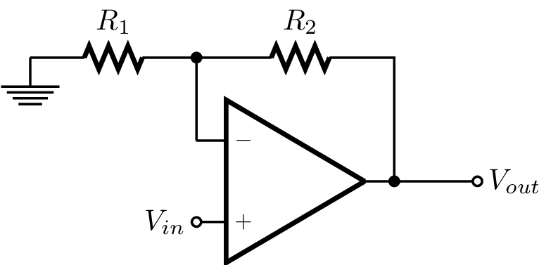
Non-Inverting Op Amp
The closed loop gain of a Non Inverting Op Amp is
- (ii)
The input impedance of this configuration is Zin = ∞ (realistically, the input impedance of the op-amp itself, 1 MΩ to 10T Ω).
Ideal Op Amp Derivation
Take a KVL with the inputs of the Op Amp and R1.
But is zero since the Op Amp is ideal. Therefore
- (3)
According to voltage divider rule
- (4)
Substitute equation 4 into 3.
Thus
Feedback Analysis Derivation
If the output is connected to the inverting input, after being scaled by a voltage divider K = R1 / (R1 + R2), then:
- V+ = Vin
- V− = K Vout
- Vout = G(Vin − K Vout)
Solving for Vout / Vin, we see that the result is a linear amplifier with gain:
- Vout / Vin = G / (1 + G K)
If G is very large, Vout / Vin comes close to 1 / K, which equals 1 + (R2 / R1).
This negative feedback connection is the most typical use of an op-amp, but many different configurations are possible, making it one of the most versatile of all electronic building blocks.
When connected in a negative feedback configuration, the op-amp will tend to output whatever voltage is necessary to make the input voltages equal. This, and the high input impedance, are sometimes called the two "golden rules" of op-amp design (for circuits that use feedback):
- No current will flow into the inputs
- The input voltages will be equal to each other
The exception is if the voltage required is greater than the op-amp's supply, in which case the output signal stops near the power supply rails, VS+ or VS−.
Example 3
Design a Non-Inverting Amplifier to amplify a 100mV signal to 1V signal. Assume: No source impedance.
Step 1: Work out required gain.
Step 2: Select an value.
- Choose .
Step 3: Work out the required value of using equation (ii).
Example 4 (a quick design procedure):
I want to amplify a signal A with a gain of 8. We want an output swing of at least -3 to +3 V.
We have a 5V and -5V power supply handy, so we can use that.
1. gain of 8 for A.
2. Ground gain = 1 - (8) = -7.
3. feedback-resistor value: Rf = 100 kiloOhms.
4. resistor values for each input:
- RA = 100 kΩ / 8 = 12.5 kΩ
- Rground = 100 kΩ / | -7 | = 14.3 kΩ
Since A has a positive gain, connect its resistor to V+. Since ground has a negative gain, connect its resistor to V−
Example 5
Design a two stage Non-Inverting Amplifier to amplify a 10mV signal to 1V signal. The signal has a source impedance of 100 Ω.
Solution Assuming an ideal Op Amp. Since this configuration has the input impendance of the Op Amp itself. We do not have to worry about loading since the input impedance is infinite.
Step 1: Work out the required gain.
Step 2: Choose the gain for each stage.
- Choose 10 for both stages.
Step 3: Choose a value for the resistors in both stages.
- Choose 90kΩ for both.
Step 4: Work out the value of .
- Using equation (ii) .
Advanced Op-Amp Configurations
The following configurations are all combinations of the Inverting and Non-Inverting Configurations or are special cases of them.
Voltage Follower
This configuration is also known as the unity gain Buffer. Since it can be used to counter the effects of loading of the source.
This configuration provides an input impedance even higher than a normal Non-Inverting since the gain reduces that input impedance. The gain is given by equation (ii). But R_2 is short circuited and R_1 is an open circuit.
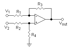
Difference amplifier
This configuration is just an Inverting and a Non-Inverting configuration connected simultaneously. Resistors R2 and R4 are a voltage divider. Consider the situation when R4 is open circuited and R2 is short circuited. Now from equations (i) and (ii) we know that the gain of V1 is
and the gain of V2 is
Now if we set to -10 then will be 11. This means that Vout will be
This means that if that Vout will be V2. This is not very useful for the most because mathematically we would like the answer to be zero. But if we make the voltage at the non-inverting input equal to 10/11 then when the voltages are equal we will have zero.
When R4 and R2 are connected the gain of V2 is
- (x)
The gain of V1 is
- (y)
If we want
We just set and .
This configuration has a low input impedance. The input impedance seen by V1 is R1 as in the Inverting Amplifier. The input impedance seen by V2 is R2 + R4.
Example 6 (a quick design procedure):
We often want to subtract one signal A from another signal B, and amplify the difference by 10. We want an output swing at least -6V to +6V. Oh, and for safety reasons, A and B each have a source impedance of 8 kΩ.
Our 5V and -5V power supply isn't adequate, so we pick a +12V and -12V power supply.
1.
- gain of +10 for B.
- gain of -10 for A.
2. Ground gain = 1 - ( +10 + -10 ) = +1.
3. feedback-resistor value: Rf = 100 kiloOhms.
4. resistor values for each input:
- RA = 100 kΩ / | -10 | = 10 kΩ
- RB = 100 kΩ / | +10 | = 10 kΩ
- Rground = 100 kΩ / | +1 | = 100 kΩ
So we connect the 100 kΩ Rf from Vout to V−, another 100 kΩ from ground to V+. Then we connect a 2 kΩ from RA to V−, and another 2 kΩ from RB to V+.
If the input has a source impedance, the source impedance is part of the circuit. The 8 kΩ source impedance, plus the 2 kΩ physical resistors we added, give us a total of 10 kΩ between the ideal voltage source and the op amp input.
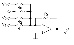
Summing amplifier
This is merely an Inverting Amplifier with extra inputs. The analysis is nearly identical but we have many currents equal to the feedback current. If we take a KCL at the Inverting input.
The value of the currents can be determined by Ohm's Law using the fact that vd is zero for an ideal Op Amp.
If then
Just as it is for the Inverting Amplifier.
Note: There is also a Summing Amplifier made using the Non-Inverting Amplifier configuration. The configuration is a bit more complicated and harder to use. Since it requires and understanding of Superposition.
Integrator
The configuration is an Inverting Amplifier with the feedback resistor a Capacitor. The derivation procedes the same.
Integrate both sides with respect to
Practically a Resistor is often connected in parallel with the feedback capacitor. This means that there is not infinite gain at very low frequencies, which makes the Integrator much more stable.
Differentiator
The configuration is an Inverting Amplifier with a Capacitor as Resistor one so the derivation proceeds the same as before.
This configuration is unstable for several reasons. The higher frequency inputs are going to have higher derivatives. Which means that circuit acts like a low pass filter, but more importantly this means that it will just saturate if a high frequency signal is put into the differentiator. This is also seen throught the gain.
This means high frequencies mean high gain and thus saturation.
Practically a Resistor is often connected in series with the capacitor.
Real Op Amps
Real Op Amps are (normally) built as an integrated circuit, but occasionally with discrete transistors or vacuum tubes. A Real Op Amp is an approximation of an Ideal Op Amp. This means that they do not have infinite open loop gain, infinite input impedance nor zero output impedance. Real Op Amps also create noise in the circuit, have an offset voltage, thermal drift and finite bandwidth.
An offset voltage means that there exists a voltage vd when both inputs are grounded. This offset is called an input offset because the voltage vd is offset from its ideal value of zero volts. The input offset voltage is multiplied by the open loop gain to create an output offset voltage.
Thermal drift means that the characteristics of the Op Amp change with temperature. That is the open loop gain, input and output impedances, offset voltages and bandwidth change as the temperature changes.
Op Amps are made up of transistors. Transistors can only respond at a certain rate because of certain capacitances that they have. This means that the Op Amps cannot respond fast enough to frequencies above a certain level. This level is the bandwidth.
Modern integrated circuit MOSFET op-amps approximate closer and closer to these ideals in limited-bandwidth, large-signal applications at room temperature. When the approximation is reasonably close, we go ahead and call the practical device an 'op-amp', forget its limitations and use the thinking and formulae given in this article.
DC Behaviour
Open-loop gain is defined as the amplification from input to output without any feedback applied. For most practical calculations, the open-loop gain is assumed to be infinite; in reality, however, it is limited by the amount of voltage applied to power the operational amplifier, i.e. Vs+ and Vs- in the above diagram. Typical devices exhibit open loop DC gain ranging from 100,000 to over 1 million. This allows the gain in the application to be set simply and exactly by using negative feedback. Of course theory and practice differ, since op-amps have limits that the designer must keep in mind and sometimes work around.
AC Behaviour
The op-amp gain calculated at DC does not apply at higher frequencies. This effect is due to limitations within the op-amp itself, such as its finite bandwidth, and to the AC characteristics of the circuit in which it is placed. The best known stumbling-block in designing with op-amps is the tendency for the device to resonate at high frequencies, where negative feedback changes to positive feedback due to parasitic lowpasses.
Typical low cost, general purpose op-amps exhibit a gain bandwidth product of a few MHz. Specialty and high speed op-amps can achieve gain bandwidth products of 100s of MHz.
Applications
- audio and video pre-amplifiers and buffers
- voltage comparators
- differential amplifiers
- differentiators and integrators
- Filters
- Precision rectifiers
- voltage and current regulators
- analogue calculators
- analogue-to-digital converters
- digital-to-analogue converters
The generic op-amp has two inputs and one output. (Some are made with floating, differential outputs.) The output voltage is a multiple of the difference between the two inputs:
floating outputs? Are you perhaps misunderstanding "fully differential amplifier" ?
- Vout = G(V+ − V−)
G is the open-loop gain of the op-amp. The inputs are assumed to have very high impedance; negligible current will flow into or out of the inputs. Op-amp outputs have very low source impedance.
If an Operational Amplifier is used with positive feedback it can act as an oscillator.
Other Notation
The power supply pins (VS+ and VS−) can be labeled many different ways. For FET based op-amps, the positive, common drain supply is labeled VDD and the negative, common source supply is labeled VSS. For BJT based op-amps, the VS+ pin becomes VCC and VS− becomes VEE. They are also sometimes labeled VCC+ and VCC−, or even V+ and V−, in which case the inputs would be labeled differently. The function remains the same.
Oscillators
When used with specific positive feedback, an Op Amp can act as an oscillator. Instances of this are:
Fully Differential Amplifier
Integrated Fully Differential Amplifier
... insert drawing of internal structure here ...
The generic op-amp has two inputs and one output.
Like an instrumentation amplifier, a fully differential amplifier (FDA) has 3 inputs.
Unlike any of the previous single-output amplifiers mentioned before, a fully differential amplifier has 2 outputs. This makes it ideal for driving w:differential signaling wire pairs and the differential inputs of some ADCs. (ADCs with 16 or more bits of precision almost always have differential inputs).
Basic Applications
... insert drawings of basic FDA amplifying circuits here ...
Fully Differential Amplifier versus Instrumentation Amplifier
An instrumentation amplifier has extremely high input impedance-- much higher than the input impedance of a fuly differential amplifier (once all the feedback resistors are in place). So an instrumentation amplifier is better for measuring voltage inputs with unknown (and possibly time-varying) output resistance.
A fully differential amplifier is better than an instrumentation amplifier for precisely generating differential output voltages, with good rejection of differential noise on the input, output, and power lines.
Applying a Quick Design Procedure
Can we apply Dieter's procedure to a fully differential amplifier? We can, if we revise it a little:
- Daisy's theorem revised:
- The sum of the gains = 0 in a properly-designed fully differential amplifier circuit.
Here is the FDA quick design procedure:
- Use equal feedback resistors Rf, one from the + output to the - input, and one from the - output to the + input. Connect the "common" input to the appropriate voltage source.
- The sum of the gains = zero in a properly-designed fully differential amplifier circuit (note that this new formulation differs from Daisy's theorem, which claims that the sum is always 1).
- Calculate resistor values for each input, using Ri = Rf / |desired gain|.
- For inputs with positive gain, connect the calculated resistor value between that input and the + input on the amplifier.
- For inputs with negative gain, connect the calculated resistor value between that input and the - input on the amplifier.
- If all your inputs are differential pairs, then the sum of all the gains is now zero. Done. Otherwise add a ground resistor to bring the total gain to zero.
Example 7 (a classic design procedure):
Example 8 (a quick design procedure):
References
- ↑ Single-formula technique keeps it simple - EDN's article by Dieter Knollman, PhD, Lucent Technologies
- ↑ K9 analysis make analog circuit design and analysis doggone simple
- ↑ How to Simplify the Design of the Mixed Op-amp Voltage Summer (after EDN's Single-formula technique keeps it simple)
See also
Further reading
- Linear Databook published in 1982 by The National Semiconductor Corporation.


